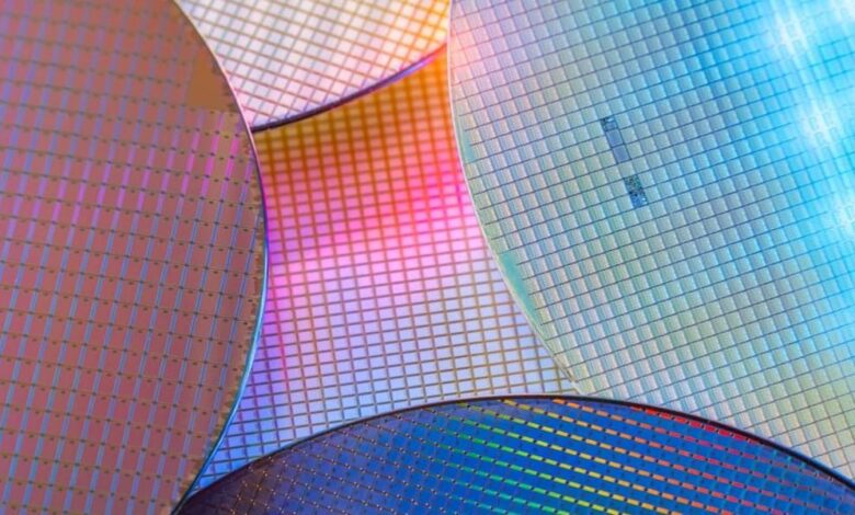
Si Wafers are thin slices of crystallised silicon that are highly pure. Due to their affordability and conductivity, silicon wafers serve as a substrate for microelectronic devices and are particularly helpful when constructing electronic circuits. The second most frequent element on earth and the seventh most frequent element in the universe belong to silicon. Beach sand, quartz, flint, agate, and other materials are common substances containing silicon. Brick, cement, and glass are prominent construction materials containing silicon.
Silicon crystals may appear metallic, yet they may not consist of metals. Metals are good conductors of electricity because “free electrons” may easily travel between atoms. Electricity is the movement of electrons. Pure patterned silicon wafers are almost an insulator while allowing very little energy to travel through them. Doping is a method through which this can be altered.
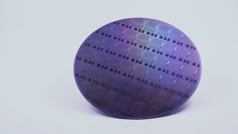
Silicon Wafer Processing
Silicon wafer processing involves various steps. The process begins with coating the silicon wafer with thin glass and nitride layers.
1. Photolithography
Photolithography is a vital step in producing patterned wafers, which enables the large-scale generation of exact patterns. Starting with a clean surface ensures the absence of impurities that can interfere with the pattern reproduction. The wafer is then evenly covered with a thin layer of photoresist. The disc is under UV light through a mask to define the patterns. The UV light selectively exposes the photoresist in particular places, while the mask includes the desired design. The exposed photoresist goes through a chemical change that makes it more or less soluble in a developer solution.
2. Direct Wafer Stepping
A stepper, used to produce integrated circuits (ICs), works similarly to a slide projector or an enlarger for photos. Step-and-repeat cameras are referred to as steppers. Steppers are a crucial component of the intricate photolithography process, producing millions of minuscule circuit parts on the surface of silicon wafers, the raw chip material. These chips are the brains of integrated circuits (ICs), which include memory chips, processors, and many other components.
3. Etching
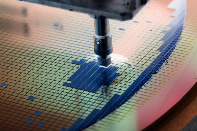
Etching is a common technique in microfabrication. It involves eliminating one or more layers to remove undesirable elements from the wafer’s surface. Semiconductor makers frequently use wet etching and dry etching to complete the task. This process makes the wafer free of any foreign materials.
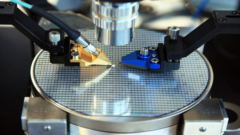
4. Masking
An opaque plate with translucent regions that let light pass through in a certain pattern is called a photomask. When creating integrated circuits (ICs, sometimes called “chips”) via photolithography, photomasks are frequently employed to create a design on a thin wafer of material, typically silicon. Each mask is applied in turn, replicating a layer of the final design, and together, they are referred to as a mask set.
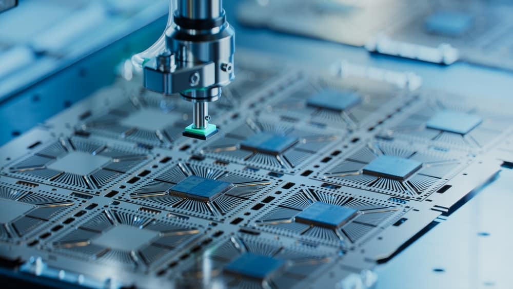
5. Wire Bonding
Wire bonding connects silicon chips and semiconductors (or other integrated circuits) electrically using tiny wires called bonding wires composed of metals like gold and aluminium. The two most popular procedures are aluminium wedge and gold ball bonding.
6. Encapsulation
Encapsulation is encasing a die in a protective coating after it has died and the wire is connected. Encapsulation serves as a shield between the semiconductor die and its wire bonds and their operational environment. Moisture, dust, dirt, solvents, mechanical straining, and scratching are potential causes of die damage. Epoxy, sealants, and additives may be used separately or in combination as part of an encapsulating deposition.
Applications Of Silicon Wafer
The applications of the silicon wafer are listed below:
1. Semiconductors
Semiconductors are the fundamental components of a wide variety of electronic devices and come in various sizes and shapes. Transistors, diodes, and integrated circuits are examples of these. They are produced using silicon wafers, contributing to their efficiency and compactness. They are utilised in optical sensors, power devices, and even lasers because of their capacity to withstand a broad range of voltage or current.
2. Optics
Polished silicon wafers are frequently produced specifically for optical grading. Silicon wafers are the ideal, cost-effective material for reflective optics and infrared (IR) technology. Silicon wafers for optics are produced using Floating Zone or CZ manufacturing techniques. This is so that the approaches outperform other methods and produce fewer flaws. All around the world, use is present in fibre optic and micro-optic devices. The complementary metal-oxide-semiconductor (CMOS) image sensors (CIS) used in cameras are a good example.
3. Electronic Devices
The semiconductors used to create chips and microchips for electrical devices are silicon wafers. These semiconductors are used to construct integrated circuits because of the characteristics of electricity flowing through silicon wafers. The integrated circuits are used as the commands for certain tasks that the electronic devices carry out in various electronic gadgets.
4. Photonics
SOI wafers are utilised in silicon photonics. The crystalline silicon layer on the insulator can create active or passive optical devices and optical waveguides through the proper implantations. Based on total internal reflection, the buried insulator allows infrared light to pass through the silicon layer. The top surface of the waveguides is covered by cladding made of silica, which can either cover it or leave it open to the air.
5. Aerospace
Aircraft original equipment manufacturing (OEM), repair, maintenance, and overhaul greatly benefit from silicon wafers. Aircraft need to be replaced because of wear and tear brought on their regular use. Because they are provided in dual cartridges and tubes, silicon wafers are useful because they save time and minimise waste.
Conclusion
Almost every aspect of modern life and technological growth uses silicon wafers. Silicon wafers are the most often utilised materials in the technology industry because they are more stable than other semiconductor materials. In addition to offering a superior alternative to other metallic materials, they are widely distributed worldwide. Technology has advanced greatly due to the research and development of semiconductor materials, including silicon, silicon carbide (SiC), germanium, arsenide, and gallium.